John Luciani
2008-03-25 22:07:19 UTC
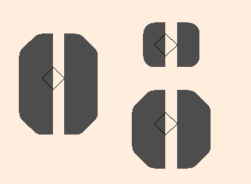
In Eagle there are a couple of solder-jumper footprints. To jumper between pads
you create a solder bridge. The two pad jumper looks like two half
circles with a
gap in between. The three pad jumper consists of a half circle on each
end with a rectangular pad in between.
I am looking for the dimensions of the pads and gaps or some recommendations.
I was thinking of making 20x50 mil rectangular pads with 10 mil gaps.
Thanks.
(* jcl *)
--
http://www.luciani.org
http://www.luciani.org